Bent Patch Antenna
Setup & Simulate a bent patch antenna using a cylindrical mesh
Introduction
This tutorial covers:
Setup of a Bent Patch Antenna (see for comparison: Simple Patch Antenna)
setup of a cylindrical FDTD mesh.
Calculate the S-Parameter and input impedance
Calculate far-field pattern 2D/3D
Python Script
Get the latest version from git.
Import Libraries
import os, tempfile
from pylab import *
from mpl_toolkits.mplot3d import Axes3D

from CSXCAD import CSXCAD

from openEMS.openEMS import openEMS
from openEMS.physical_constants import *
Setup the simulation
Sim_Path = os.path.join(tempfile.gettempdir(), 'Bent_Patch')

post_proc_only = False

unit = 1e-3 # all length in mm

f0 = 2.4e9 # center frequency, frequency of interest!
lambda0 = round(C0/f0/unit) # wavelength in mm
fc = 0.5e9 # 20 dB corner frequency

# patch width in alpha-direction
patch_width  = 32 # resonant length in alpha-direction
patch_radius = 50 # radius
patch_length = 40 # patch length in z-direction

#substrate setup
substrate_epsR   = 3.38
substrate_kappa  = 1e-3 * 2*pi*2.45e9 * EPS0*substrate_epsR
substrate_width  = 80
substrate_length = 90
substrate_thickness = 1.524
substrate_cells = 4

#setup feeding
feed_pos   = -5.5  #feeding position in x-direction
feed_width = 2     #feeding port width
feed_R     = 50    #feed resistance

# size of the simulation box
SimBox_rad    = 2*100
SimBox_height = 1.5*200
Setup FDTD parameter & excitation function
FDTD = openEMS(CoordSystem=1, EndCriteria=1e-4) # init a cylindrical FDTD
f0 = 2e9 # center frequency
fc = 1e9 # 20 dB corner frequency
FDTD.SetGaussExcite(f0, fc)
FDTD.SetBoundaryCond(['MUR', 'MUR', 'MUR', 'MUR', 'MUR', 'MUR']) # boundary conditions
Setup the Geometry & Mesh
# init a cylindrical mesh
CSX = CSXCAD.ContinuousStructure(CoordSystem=1)
FDTD.SetCSX(CSX)
mesh = CSX.GetGrid()
mesh.SetDeltaUnit(unit)
Setup the geometry using cylindrical coordinates
# calculate some width as an angle in radiant
patch_ang_width = patch_width/(patch_radius+substrate_thickness)
substr_ang_width = substrate_width/patch_radius
feed_angle = feed_pos/patch_radius

# create patch
patch = CSX.AddMetal('patch') # create a perfect electric conductor (PEC)
start = [patch_radius+substrate_thickness, -patch_ang_width/2, -patch_length/2 ]
stop  = [patch_radius+substrate_thickness,  patch_ang_width/2,  patch_length/2 ]
patch.AddBox(priority=10, start=start, stop=stop) # add a box-primitive to the metal property 'patch'
FDTD.AddEdges2Grid(dirs='all', properties=patch)

# create substrate
substrate = CSX.AddMaterial('substrate', epsilon=substrate_epsR, kappa=substrate_kappa  )
start = [patch_radius                    , -substr_ang_width/2, -substrate_length/2]
stop  = [patch_radius+substrate_thickness,  substr_ang_width/2,  substrate_length/2]
substrate.AddBox(start=start, stop=stop)
FDTD.AddEdges2Grid(dirs='all', properties=substrate)

# save current density oon the patch
jt_patch = CSX.AddDump('Jt_patch', dump_type=3, file_type=1)
start = [patch_radius+substrate_thickness, -substr_ang_width/2, -substrate_length/2]
stop  = [patch_radius+substrate_thickness, +substr_ang_width/2,  substrate_length/2]
jt_patch.AddBox(start=start, stop=stop)

# create ground
gnd = CSX.AddMetal('gnd') # create a perfect electric conductor (PEC)
start = [patch_radius, -substr_ang_width/2, -substrate_length/2]
stop  = [patch_radius, +substr_ang_width/2, +substrate_length/2]
gnd.AddBox(priority=10, start=start, stop=stop)
FDTD.AddEdges2Grid(dirs='all', properties=gnd)

# apply the excitation & resist as a current source
start = [patch_radius                    ,  feed_angle, 0]
stop  = [patch_radius+substrate_thickness,  feed_angle, 0]
port = FDTD.AddLumpedPort(1 ,feed_R, start, stop, 'r', 1.0, priority=50, edges2grid='all')
Finalize the Mesh
# add the simulation domain size
mesh.AddLine('r', patch_radius+np.array([-20, SimBox_rad]))
mesh.AddLine('a', [-0.75*pi, 0.75*pi])
mesh.AddLine('z', [-SimBox_height/2, SimBox_height/2])

# add some lines for the substrate
mesh.AddLine('r', patch_radius+np.linspace(0,substrate_thickness,substrate_cells))

# generate a smooth mesh with max. cell size: lambda_min / 20
max_res = C0 / (f0+fc) / unit / 20
max_ang = max_res/(SimBox_rad+patch_radius) # max res in radiant
mesh.SmoothMeshLines(0, max_res, 1.4)
mesh.SmoothMeshLines(1, max_ang, 1.4)
mesh.SmoothMeshLines(2, max_res, 1.4)
Add the nf2ff recording box
nf2ff = FDTD.CreateNF2FFBox()
Run the simulation
if 0:  # debugging only
    CSX_file = os.path.join(Sim_Path, 'bent_patch.xml')
    if not os.path.exists(Sim_Path):
        os.mkdir(Sim_Path)
    CSX.Write2XML(CSX_file)
    from CSXCAD import AppCSXCAD_BIN
    os.system(AppCSXCAD_BIN + ' "{}"'.format(CSX_file))


if not post_proc_only:
    FDTD.Run(Sim_Path, cleanup=True)
Postprocessing & plotting
f = np.linspace(max(1e9,f0-fc),f0+fc,401)
port.CalcPort(Sim_Path, f)
Zin = port.uf_tot / port.if_tot
s11 = port.uf_ref/port.uf_inc
s11_dB = 20.0*np.log10(np.abs(s11))

figure()
plot(f/1e9, s11_dB)
grid()
ylabel('s11 (dB)')
xlabel('frequency (GHz)')

P_in = 0.5*np.real(port.uf_tot * np.conj(port.if_tot)) # antenna feed power

# plot feed point impedance
figure()
plot( f/1e6, real(Zin), 'k-', linewidth=2, label=r'$\Re(Z_{in})$' )
grid()
plot( f/1e6, imag(Zin), 'r--', linewidth=2, label=r'$\Im(Z_{in})$' )
title( 'feed point impedance' )
xlabel( 'frequency (MHz)' )
ylabel( 'impedance ($\Omega$)' )
legend( )


idx = np.where((s11_dB<-10) & (s11_dB==np.min(s11_dB)))[0]
if not len(idx)==1:
    print('No resonance frequency found for far-field calulation')
else:
    f_res = f[idx[0]]
    theta = np.arange(-180.0, 180.0, 2.0)
    print("Calculate NF2FF")
    nf2ff_res_phi0 = nf2ff.CalcNF2FF(Sim_Path, f_res, theta, 0, center=np.array([patch_radius+substrate_thickness, 0, 0])*unit, read_cached=True, outfile='nf2ff_xz.h5')

    figure(figsize=(15, 7))
    ax = subplot(121, polar=True)
    E_norm = 20.0*np.log10(nf2ff_res_phi0.E_norm/np.max(nf2ff_res_phi0.E_norm)) + nf2ff_res_phi0.Dmax
    ax.plot(np.deg2rad(theta), 10**(np.squeeze(E_norm)/20), linewidth=2, label='xz-plane')
    ax.grid(True)
    ax.set_xlabel('theta (deg)')
    ax.set_theta_zero_location('N')
    ax.set_theta_direction(-1)
    ax.legend(loc=3)

    phi = theta
    nf2ff_res_theta90 = nf2ff.CalcNF2FF(Sim_Path, f_res, 90, phi, center=np.array([patch_radius+substrate_thickness, 0, 0])*unit, read_cached=True, outfile='nf2ff_xy.h5')

    ax = subplot(122, polar=True)
    E_norm = 20.0*np.log10(nf2ff_res_theta90.E_norm/np.max(nf2ff_res_theta90.E_norm)) + nf2ff_res_theta90.Dmax
    ax.plot(np.deg2rad(phi), 10**(np.squeeze(E_norm)/20), linewidth=2, label='xy-plane')
    ax.grid(True)
    ax.set_xlabel('phi (deg)')
    suptitle('Bent Patch Anteanna Pattern\nFrequency: {} GHz'.format(f_res/1e9), fontsize=14)
    ax.legend(loc=3)

    print( 'radiated power: Prad = {:.2e} Watt'.format(nf2ff_res_theta90.Prad[0]))
    print( 'directivity:    Dmax = {:.1f} ({:.1f} dBi)'.format(nf2ff_res_theta90.Dmax[0], 10*np.log10(nf2ff_res_theta90.Dmax[0])))
    print( 'efficiency:   nu_rad = {:.1f} %'.format(100*nf2ff_res_theta90.Prad[0]/real(P_in[idx[0]])))

show()
Images
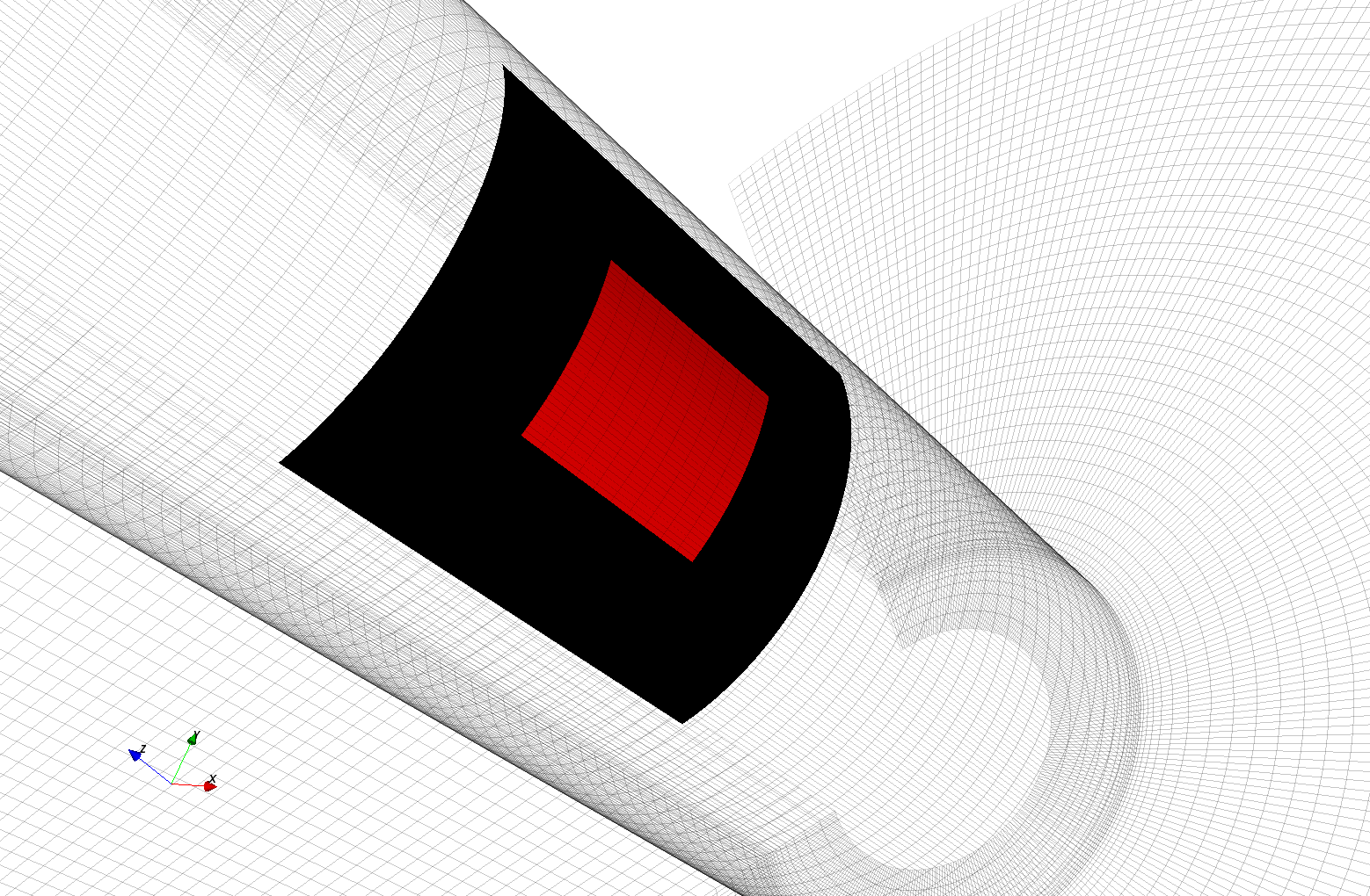
3D view of the Bent Patch Antenna (AppCSXCAD)
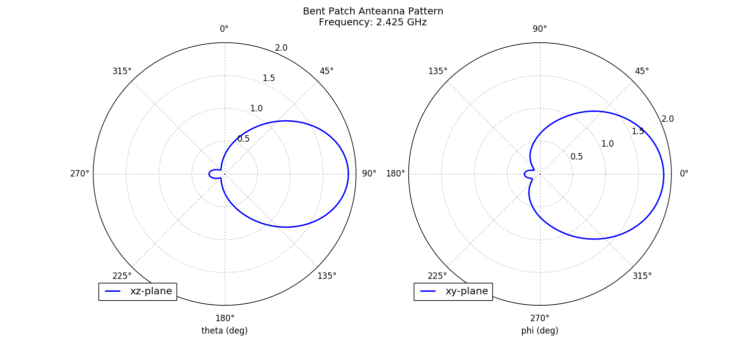
Farfield pattern on an xy- and xz-plane