Simple Patch Antenna
Introduction
A simple patch antenna for 2.4 GHz.
This tutorial covers:
Setup a patch, substrate and ground.
Setup of a lumped feeding port.
Adding a near-field to far-field (nf2ff) recording box.
Calculate the S-Parameter of the antenna.
Calculate and plot the far-field pattern
Python Script
Get the latest version from git.
Import Libraries
import os, tempfile
from pylab import *

from CSXCAD  import ContinuousStructure
from openEMS import openEMS
from openEMS.physical_constants import *
General parameter setup
Sim_Path = os.path.join(tempfile.gettempdir(), 'Simp_Patch')

post_proc_only = False

# patch width (resonant length) in x-direction
patch_width  = 32 #
# patch length in y-direction
patch_length = 40

#substrate setup
substrate_epsR   = 3.38
substrate_kappa  = 1e-3 * 2*pi*2.45e9 * EPS0*substrate_epsR
substrate_width  = 60
substrate_length = 60
substrate_thickness = 1.524
substrate_cells = 4

#setup feeding
feed_pos = -6 #feeding position in x-direction
feed_R = 50     #feed resistance

# size of the simulation box
SimBox = np.array([200, 200, 150])

# setup FDTD parameter & excitation function
f0 = 2e9 # center frequency
fc = 1e9 # 20 dB corner frequency
FDTD setup
Limit the simulation to 30k timesteps
Define a reduced end criteria of -40dB
FDTD = openEMS(NrTS=30000, EndCriteria=1e-4)
FDTD.SetGaussExcite( f0, fc )
FDTD.SetBoundaryCond( ['MUR', 'MUR', 'MUR', 'MUR', 'MUR', 'MUR'] )


CSX = ContinuousStructure()
FDTD.SetCSX(CSX)
mesh = CSX.GetGrid()
mesh.SetDeltaUnit(1e-3)
mesh_res = C0/(f0+fc)/1e-3/20
Generate properties, primitives and mesh-grid
#initialize the mesh with the "air-box" dimensions
mesh.AddLine('x', [-SimBox[0]/2, SimBox[0]/2])
mesh.AddLine('y', [-SimBox[1]/2, SimBox[1]/2]          )
mesh.AddLine('z', [-SimBox[2]/3, SimBox[2]*2/3]        )

# create patch
patch = CSX.AddMetal( 'patch' ) # create a perfect electric conductor (PEC)
start = [-patch_width/2, -patch_length/2, substrate_thickness]
stop  = [ patch_width/2 , patch_length/2, substrate_thickness]
patch.AddBox(priority=10, start=start, stop=stop) # add a box-primitive to the metal property 'patch'
FDTD.AddEdges2Grid(dirs='xy', properties=patch, metal_edge_res=mesh_res/2)

# create substrate
substrate = CSX.AddMaterial( 'substrate', epsilon=substrate_epsR, kappa=substrate_kappa)
start = [-substrate_width/2, -substrate_length/2, 0]
stop  = [ substrate_width/2,  substrate_length/2, substrate_thickness]
substrate.AddBox( priority=0, start=start, stop=stop )

# add extra cells to discretize the substrate thickness
mesh.AddLine('z', linspace(0,substrate_thickness,substrate_cells+1))

# create ground (same size as substrate)
gnd = CSX.AddMetal( 'gnd' ) # create a perfect electric conductor (PEC)
start[2]=0
stop[2] =0
gnd.AddBox(start, stop, priority=10)

FDTD.AddEdges2Grid(dirs='xy', properties=gnd)

# apply the excitation & resist as a current source
start = [feed_pos, 0, 0]
stop  = [feed_pos, 0, substrate_thickness]
port = FDTD.AddLumpedPort(1, feed_R, start, stop, 'z', 1.0, priority=5, edges2grid='xy')

mesh.SmoothMeshLines('all', mesh_res, 1.4)

# Add the nf2ff recording box
nf2ff = FDTD.CreateNF2FFBox()
Run the simulation
if 0:  # debugging only
    CSX_file = os.path.join(Sim_Path, 'simp_patch.xml')
    if not os.path.exists(Sim_Path):
        os.mkdir(Sim_Path)
    CSX.Write2XML(CSX_file)
    from CSXCAD import AppCSXCAD_BIN
    os.system(AppCSXCAD_BIN + ' "{}"'.format(CSX_file))

if not post_proc_only:
    FDTD.Run(Sim_Path, verbose=3, cleanup=True)
Post-processing and plotting
f = np.linspace(max(1e9,f0-fc),f0+fc,401)
port.CalcPort(Sim_Path, f)
s11 = port.uf_ref/port.uf_inc
s11_dB = 20.0*np.log10(np.abs(s11))
figure()
plot(f/1e9, s11_dB, 'k-', linewidth=2, label='$S_{11}$')
grid()
legend()
ylabel('S-Parameter (dB)')
xlabel('Frequency (GHz)')

idx = np.where((s11_dB<-10) & (s11_dB==np.min(s11_dB)))[0]
if not len(idx)==1:
    print('No resonance frequency found for far-field calulation')
else:
    f_res = f[idx[0]]
    theta = np.arange(-180.0, 180.0, 2.0)
    phi   = [0., 90.]
    nf2ff_res = nf2ff.CalcNF2FF(Sim_Path, f_res, theta, phi, center=[0,0,1e-3])

    figure()
    E_norm = 20.0*np.log10(nf2ff_res.E_norm[0]/np.max(nf2ff_res.E_norm[0])) + nf2ff_res.Dmax[0]
    plot(theta, np.squeeze(E_norm[:,0]), 'k-', linewidth=2, label='xz-plane')
    plot(theta, np.squeeze(E_norm[:,1]), 'r--', linewidth=2, label='yz-plane')
    grid()
    ylabel('Directivity (dBi)')
    xlabel('Theta (deg)')
    title('Frequency: {} GHz'.format(f_res/1e9))
    legend()

Zin = port.uf_tot/port.if_tot
figure()
plot(f/1e9, np.real(Zin), 'k-', linewidth=2, label='$\Re\{Z_{in}\}$')
plot(f/1e9, np.imag(Zin), 'r--', linewidth=2, label='$\Im\{Z_{in}\}$')
grid()
legend()
ylabel('Zin (Ohm)')
xlabel('Frequency (GHz)')

show()
Images
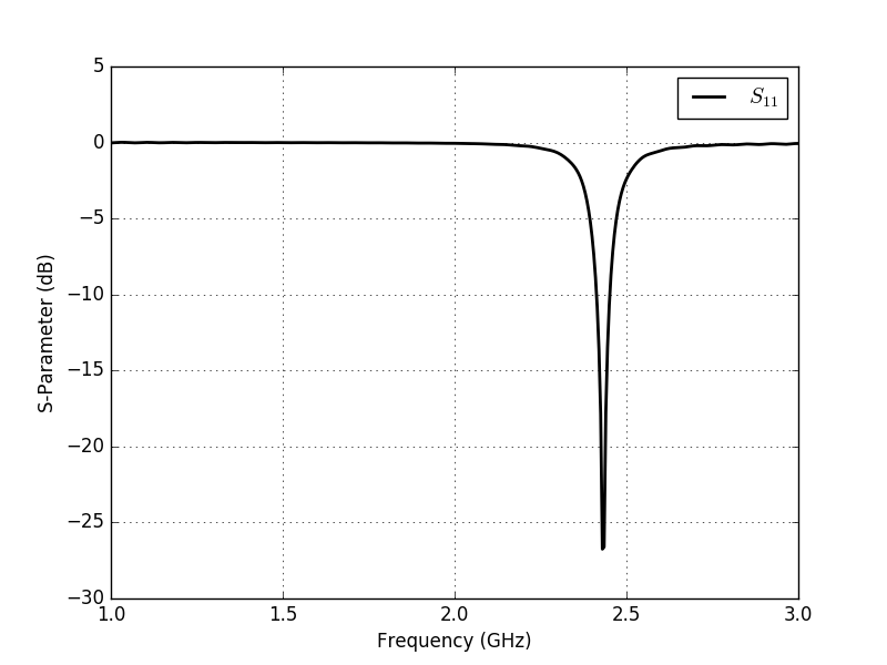
S-Parameter over Frequency
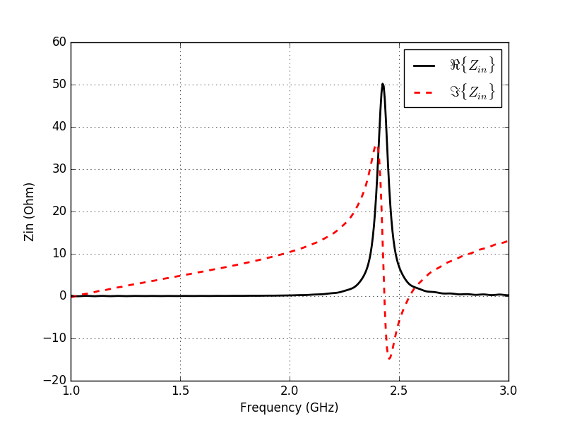
Antenna Input Impedance
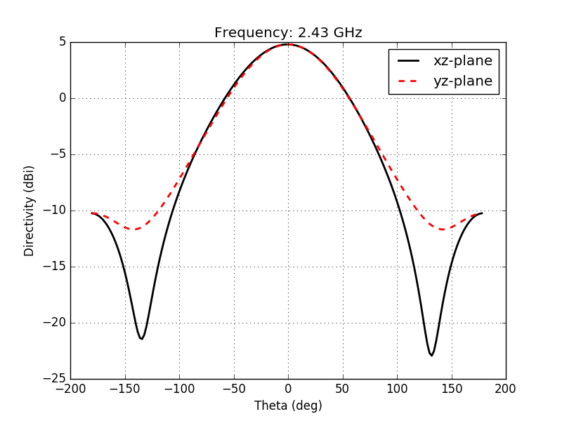
Farfield pattern for the xy- and yz-plane.